Semiconductors Part 2: Doping & Types of Semiconductor
 |
| Guillom assumed (based on copyright claims): https://commons.wikimedia.org/wiki/File:N-doped_Si.svg |
In Part 1 (https://phys-talk.blogspot.com/2020/07/semiconductors-part-1-introduction-band.html), we looked at the basics of semiconductors,
using band theory to visualise how they differ from insulators and conductors.
From Part 1, we learned that silicon is classed as a semiconductor due to the small energy gap between the valence and conduction bands. However, the conductivity of pure silicon is low and therefore it is not very useful in electronics. Doping is a method implemented to alter the properties of a semiconductor and modify its conductivity. It involves adding impurities to an intrinsic semiconductor (like silicon) to ‘generate either a surplus or a deficiency in valence electrons.’ [1] This imbalance allows for the movement of electrons through the material and therefore current can flow.
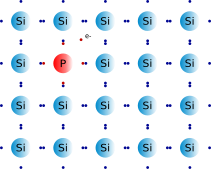
N-type
semiconductors

This diagram shows the structure of doped Silicon: Phosphorus, which has five outer electrons has been added. As you can see four of these valence electrons form covalent bonds with the four outer electrons of the Silicon atoms. This leaves one free electron per Phosphorus atom which is not bonded (shown in yellow). When connected to a power source, this free electron is attracted to the positive terminal and is free to move. Thus, charge can flow generating electric currents. This is an example of an N-type semiconductor.
P-type semiconductors

This is also an example of doped Silicon. However, this time, Boron has been introduced instead of Phosphorus. Boron has 3 electrons in its outer shell. As a result, it only has enough valence electrons to covalently bond to three of the four surrounding Silicon atoms. The dashed black circle represents a hole where an electron would normally be in a pure Silicon crystal. If a voltage is applied, electrons nearby can fill this hole. This in turn creates a new hole which can be filled by another electron. Overall, the electrons move via the holes towards to positive terminal. This results in the holes moving in the opposite direction, towards the negative terminal. This is called a P-type semiconductor.
Naming
To sum up, N-type semiconductors result from a surplus of
electrons in the material. They are named as such because the motion of negative
electrons is what allows current to flow. Meanwhile, P-type semiconductors involve
a deficiency in valence electrons which leaves holes. These holes have the
effect of a positive charge as they travel towards the negative terminal. This explains
why they are called P-type semiconductors: current flows due to the motion of
holes which are positive charge carriers.
Quasiparticles
Holes due to the absence of an electron are examples of
quasiparticles. A quasiparticle is a ‘disturbance […] that behaves as a particle
and that may conveniently be regarded as one.’ [2]
Sources:
1. Lumen: https://courses.lumenlearning.com/introchem/chapter/doping-connectivity-of-semiconductors/
2. Encyclopædia Britannica: https://www.britannica.com/science/quasiparticle
Khan Academy: https://www.youtube.com/watch?v=60Qz051rD_w&t=369s
Comments
Post a Comment